Der Inhalt dieser Seite ist leider nur auf Englisch verfügbar.
Surface metallicity in iron silicide
High mobility surface conduction due to interfacial symmetry breaking
2021-11-25 – News from the Physics Department
Semiconductors are important materials for all kinds of modern electronic devices, including amplifiers and computer chips. This usefulness is due to their distinctive electrical properties. The electrical conductivity value of semiconductors falls between that of conductors, such as metallic copper and insulators such as glass or porcelain. Moreover their resistivity generally falls as the temperature rises, which is the opposite behavior of metals. Semiconductor devices can display a range of useful properties, such as passing current more easily in one direction than the other or showing variable resistance.
For semiconductors, thermally activated charge carriers become quenched at low temperatures. This causes the well-understood increase of several orders of magnitude of the electrical resistivity when temperature approaches absolute zero.
In contrast to this, for a class of so-called correlated narrow-gap semiconductors, the resistivity deviates from such an activated behavior and tends to saturate at low temperatures, suggesting the emergence of some form of metallic conduction. This has been attributed to many-body effects that could play an important role in these type of semiconductors.
For the prototypical d-electron narrow-gap semiconductor iron monosilicide (FeSi), the putative presence of low-temperature metallic behavior has been a puzzle for many decades. Indeed, to reconcile the coexistence of insulating and metallic behavior at low temperatures, it is widely believed that impurities embedded in the bulk of the material represent the source of a low concentration of itinerant charge carriers.
Seeing is believing
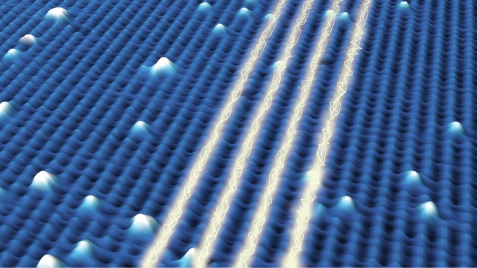
“Based on the Hall effect we have long speculated that there may be a surface conduction channel at low temperatures in FeSi,” says Dr. Andreas Bauer, who coordinated both the growth of ultrahigh purity FeSi single crystals and the conventional electrical transport measurements. “It is particularly unusual that the surface conduction channel of FeSi exhibits such a very high electron mobility, comparable to that of topological insulators, and yet appears to be insensitive to the presence of ferromagnetic impurities,” explains Prof. Christian Pfleiderer, chair of Topology of Correlated Systems.
To tackle the mystery, the FeSi single crystals were investigated at the facilities of the chair of Surface and Interface Physics of Prof. Johannes Barth, operating a wide range of sophisticated characterization tools. Researchers there were ready to take on the challenge, to visualize for the first time the atomic structure of the high-purity FeSi surface. “It took us quite some time to figure out how to prepare atomically flat surfaces in ultrahigh vacuum, which is necessary for scanning tunneling microscopy (STM) and spectroscopy (STS). But it was well worth the effort,” recall Dr. Biao Yang and Dr. Martin Uphoff, who conducted the STM and STS measurements. “We indeed explored the low-temperature metallic state on the FeSi surface. To our surprise, it appears on perfectly ordered terraces and remains largely affected by the adatoms, defects or step edges,” explains Dr. Yiqi Zhang, who was leading this campaign.
As the STM/STS results clearly show that surface metallicity is not related to the impurities, the research teams at TUM sought the theoretical support of Dr. Ari Seitsonen, an expert for computational modeling and density functional theory (DFT) at École Normale Supérieure in Paris, trying to understand the underlying mechanisms. “The DFT calculations show that FeSi does have a small bulk energy gap, which, however, gets filled once the surface-vacuum boundaries are included in the modeling. This naturally gives rise to the surface-related electronic bands crossing the bulk gap.”
A promising material
“It’s a beautiful interdisciplinary team effort and an important breakthrough!” says Prof. Johannes Barth. He explains further: “There are interesting open questions remaining, for example, is the surface metallic state topologically nontrivial? Or is there perhaps magnetic order at the surface of FeSi, which is actually non-magnetic in the bulk? Another intriguing part of this material concerns the chiral crystal structure of FeSi, which might have a profound influence on the interfacial electrical transport and we don’t know yet in which way”. “It is feasible to integrate FeSi into silicon-based electronics via interfacial engineering. To exploit low-dissipation surface conduction is of great technological relevance for reducing the power consumption of devices,” adds surface physicist Joachim Reichert.
Publication
More information
This research was supported by the German Research Foundation (DFG) through the Excellence Clusters Munich Center for Advanced Photonics (MAPS) and Munich Centre for Quantum Science and Technology (MCQST), the TUM Institute of Advanced Studies, and the Munich Quantum Center, as well as the European Research Council and the DFG Corporate Research Center TRR80. Biao Yang acknowledges the TUM University Foundation and the Alexander von Humboldt-Foundation for a Research Fellowship for Postdoctoral Researchers.
Contact
- Prof. Dr. Johannes V. BarthTel.: +49 89 289 12616 – E-Mail: jvb@tum.de
- Prof. Dr. Christian PfleidererTel.: +49 89 289 14720 – E-Mail: christian.pfleiderer@tum.de