Electrons on a rapid journey through a crystal lattice
2015-01-14 – News from Physics Department
The time frames, in which electrons travel within atoms, are unfathomably short. For example, electrons excited by light change their quantum-mechanical location within mere attoseconds. An attosecond corresponds to a billionth of a billionth of a second.
But how fast do electrons whiz across distances corresponding to the diameter of individual atomic layers? Such distances are but a few billionths of a metre. An international team of researchers led by Reinhard Kienberger, Professor for Laser and X-Ray Physics at the TUM and Head of a Research Group at the Max Planck Institute of Quantum Optics investigated the travel times of electrons over these extremely short distances.
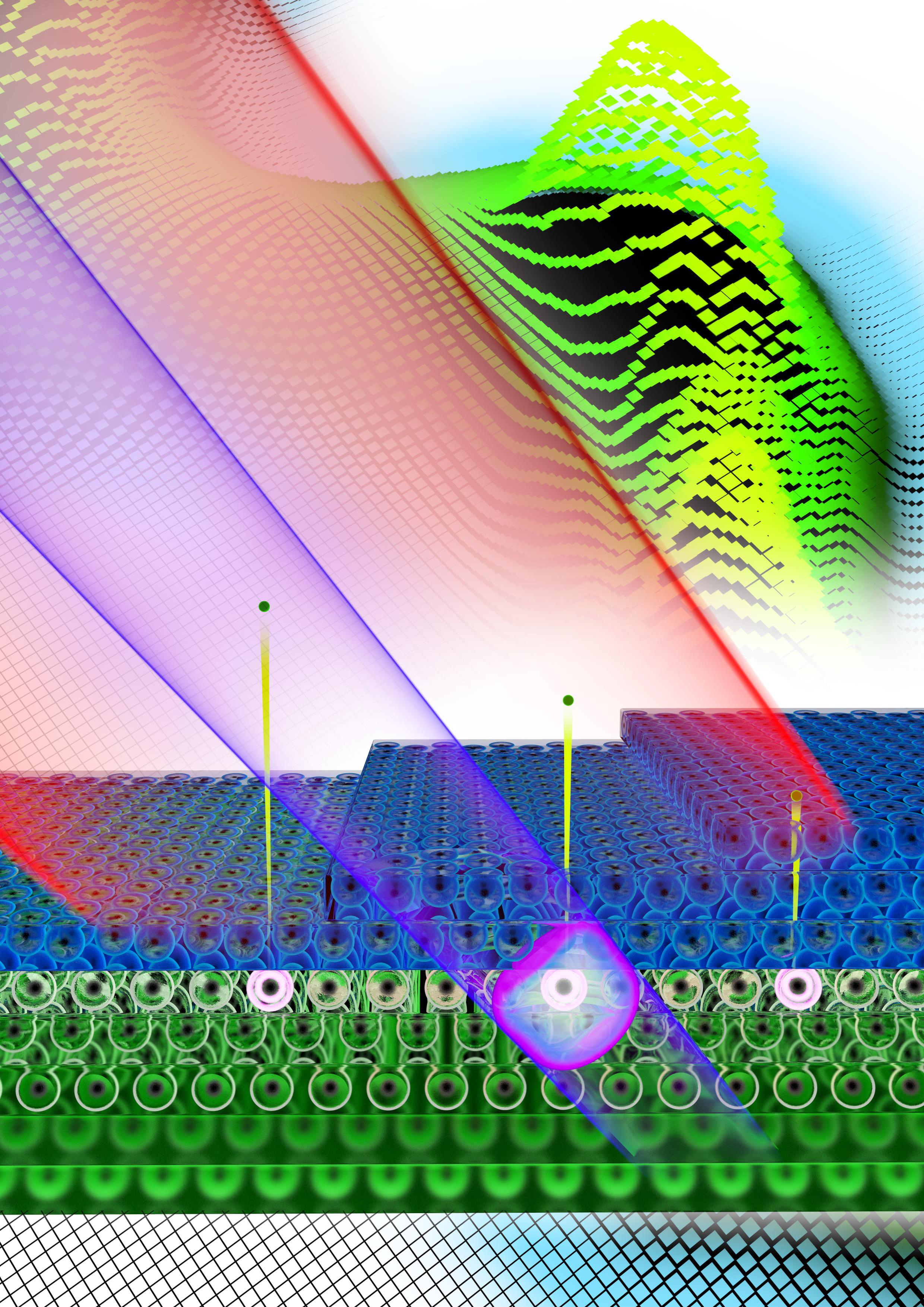
To do so, the physicists applied a defined number of layers of magnesium atoms on top of a tungsten crystal. The researchers directed two pulses of light at these samples. The first pulse lasted approximately 450 attoseconds, at frequencies within the extreme ultraviolet. This light pulse penetrated the material and released an electron from a magnesium atom in the layer system as well as from an atom in the underlying tungsten crystal. Both the electrons that were set free stemmed from the immediate vicinity of the nucleus.
Once released, the “tungsten electron” and the “magnesium electron” travelled through the crystal to the surface at which point they left the solid body. (electrons from the tungsten crystal managed to penetrate up to four layers of magnesium atoms.) There, the particles were captured by the electric field of the second pulse, an infrared wave train lasting less than five femtoseconds.
As the “tungsten electron” and the “magnesium electron” reached the surface at different times due to different path lengths, they experienced the second pulse of infrared light at different times. That is, they were exposed to different strengths of the oscillating electric field. As a result, both particles were accelerated to varying degrees. From the resulting differences in the energy of the electrons, the researchers were able to determine how long an electron needed to pass through a single layer of atoms. The measurements showed that upon release a “tungsten electron” possesses a speed of about 5000 kilometers per second. When travelling through a layer of magnesium atoms it is delayed by approximately 40 attoseconds, i.e., this is exactly the time required to travel through this layer.
The experiments provide insight into how electrons move within the widely unknown microcosm. Knowing how fast an electron travels from one place to the next is of substantial importance for many applications: “While a large number of electrons are able to cover increasingly large distances in today’s transistors, for example, individual electrons could transmit a signal through nanostructures in future”, explains Prof. Reinhard Kienberger. “As a result, electronic devices like computers could be made to be several times faster and smaller.”
The research was funded by the German Research Council (DFG; via the Cluster of Excellence Munich Center of Advanced Photonics, SFB 51 and SFB 49), the Austrian Science Fonds (FWF), the Max Planck Research School of Advanced Photon Science (IMPRS-APS) an the European Research Council (ERC).
- Editing
- Thorsten Naeser (MAP), Dr. Andreas Battenberg (TUM), Dr. Johannes Wiedersich
Publication
Contact
- Prof. Dr. Reinhard Kienberger
- Technische Universität Münchenund Max-Planck-Institut für Quanten-OptikJames Frank Str.85748 GarchingTel.: +49 89 289 12840E-Mail: reinhard.kienberger@tum.de
Links
- Research group of Prof. Dr. Reinhard Kienberger